Building An FPGA Shell
At some point, for some inexplicable reason, one may have to build an FPGA shell. Actually, I would highly encourage building one if one is interested in understanding the nitty-gritty details of an FPGA. When it became time for me to do it, I was very fortunate to have a mentor right next to me, advising what the right approach is. In this process, I realized there are bespoke knowledge that one must know in order to build a successful, working FPGA shell. Here, I want to write down the lessons, both to preserve it, and to help others building their own. Instead of elaborating on the exact Vivado buttons that one has to push (this should be done yourself), I will focus more on the overall picture.
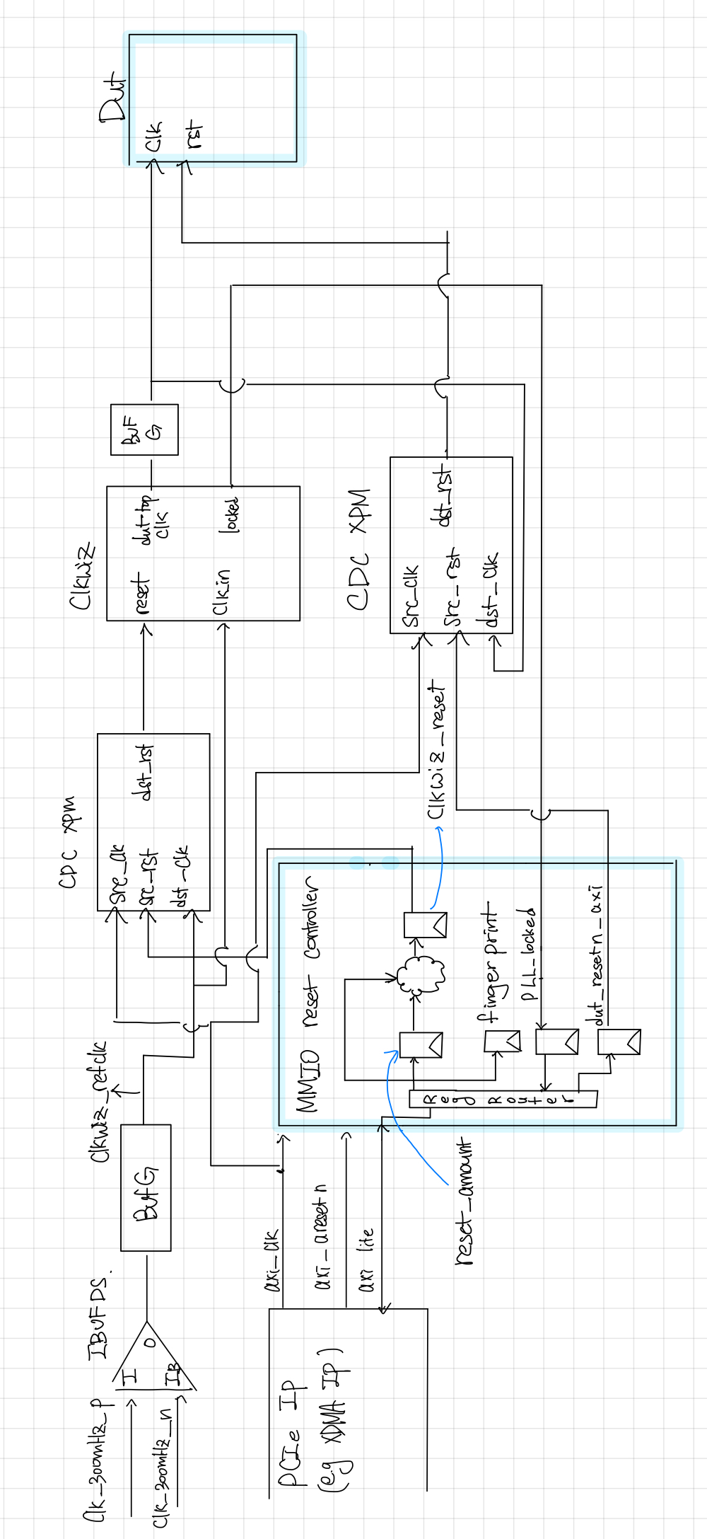
The modules colored blue are what you, as the FPGA designer must build. The rest is Xilinx IP.
Top-Level Clock, PLL, and the Reset Sequence
The top level differential clock signals (clk_300mHz_p & clk_300mHz_n) are coming from the crystal oscillator. The oscillator is just another IC on the FPGA board driving the FPGA top level I/O pins. The differential clock is passed on the IBUFDS which converts the differential clocks into a clean single-ended clock. The output of the IBUFDS drives BUFG which is a high-fanout buffer that will connect signals to global routing resources for low skew distribution (i.e., a clock network).
The output of BUFG (clkwiz_refclk) is the reference clock to the clock wizard (clkwiz). The clock wizard is another Xilinx IP that is essentially a wrapper around a PLL/MMCM.
Now, we can see that the clock wizard receives a reset signal (dst_rst) over a clock domain crossing. For single-bit clock-crossings, we can simply use the Xilinx Parameterized Macros (XPM). We can see that there is a MMIO reset controller block that has a register that drives src_rst. But what is going on in here?
To set the clock wizard (clkwiz) properly, we need to perform two things. First, we must hold the dst_rst signal going into clkwiz for a sufficient amount of time. If too short or too long, the PLL will not lock. Next, we must make sure that the locked signal, indicating that the PLL has been locked properly and is generating a clean output clock, is held high.
Ideally, we should be able to read the locked signal, control how long the reset signal must be hold high, and control the value of src_rst and the dut_resetn_axi (which will reset the DUT) in software. This enables us to have confidence that the PLL is locked. Furthermore, in cases when the PLL is not locked, we can change the reset duration and send a reset signal to clkwiz again, without having to reprogram the FPGA.
This MMIO reset controller block can be connected to the PCIe IP (e.g., the XDMA IP) and by connecting the AXI-lite signals to a register router, it can read and write to various registers inside it. The software will typically perform these operations:
- Read & write to the
fingerprintregister inside the module. This provides us confidence that the XDMA IP, and AXI-lite read and writes work as expected - Write to the
reset_amountregister which represents the duration where which theclkwiz_resetregister will be held high. This should be around 10 ~ 100 cycles for a 100MHz FPGA. If the reset signal is hold for too long, the PLL will never lock - Write to
clkwiz_reset. This will set the reset value to high, and the FSM before it will pull it down low afterreset_amountcycles - Read the
pll_lockedsignal & poll until it goes high - Once
pll_lockedgoes high, set thedut_resetn_axiwhich will reset the DUT. Having a separate reset for the DUT is important, as we don't want to start with a state where the clock could have been unstable previously
This is pretty much it. If the constraints for each IP is set correctly and you follow this reset sequence, things should hopefully work (although anything can go wrong with FPGAs).
Other Misc Tips
- After the Xilinx FPGA is programmed, all register & SRAM states are zeroed out unless specified with an initial value. This is tremendously helpful for debuging
- The clock wizard can also be configured by a MMIO register so that the generated output clock frequency can be controlled in software
- This is useful when pushing the frequency of the DUT clock as much as possible
- It's good practice to add an MMIO register that checks whether the PLL locked signal goes down after being set high. This provides further confidence that the PLL is locked properly
- The PLL locked signal is in the clock domain of the reference clock (
clkwiz_refclkin the diagram). Hence, there should be a CDC (omitted in the diagram) between thelockedsignal and thePLL_lockedMMIO register - Its good practice to flop the reset going into the dut with respect to the dut clock
- When interfacing with FPGA IO pins, its encouraged to used IOB registers (located inside an IO cell) to flop the combinational logic driving the IO pin
- Using a normal FF & routing resources can cause arbitrary delay to the IO pins, causing variability whenever a bitstream is built
- Increases the change of your design to meet timing as the IO related logic will be placed closer to the IO pin
- Why using IOB registers is a good pratice
- powerup reset sequence: this post is also a good read on the same topic