RTL Emulation
Entering the CAD business as a startup means facing a mountain of corpses, the ones who saw themselves as Davids facing Goliath, never realizing that without a slingshot they never stood a chance.
In this article, we will go over the prior and ongoing attempts to enter this market, specifically in RTL simulation and emulation1. We will also examine whether there is any opportunity in repurposing ML chips as RTL emulators. Finally, this article presents my view on what David’s slingshot would be for anyone who intends to enter battle with the incumbents.
Prior & Ongoing Companies
Let's take a look at the previous attempts at working on RTL simulation/emulation. Maybe this might reveal something we can learn from.
RocketTick
RocketTick is arguably the most successful company among the startups in this area. It was acquired by Cadence. Their goal was to accelerate RTL simulations, initially using GPUs, until they later switched to an x86 multicore platform. The GPU version is similar to Nvidia's recent publication GEM where the compiled design is taken as an input by a CUDA kernel that interprets and executes the netlist.
Nvidia was their major customer. This was not simply because RocketTick used Nvidia GPUs and achieved speedups of about 10~20X, but because the software quality was very high, especially around the test harness. RocketTick used VCS for the test harness and supported a PLI compliant interface, which meant that any non-synthesizable subset of Verilog could be extracted and run on the host CPU. It supported four-state simulation, VCD and FSDB dumping, had compilation times close to VCS, included job distribution software that could dispatch runs across a GPU cloud, and had enough simulation capacity to handle about 270 million gates. Although Nvidia relied on VCS for sign-off, they adopted RocketTick for regression runs because it was a drop-in replacement for VCS.
The reason why they moved to a multicore based simulator is unclear. If I were to guess, it is probably because they found it difficult to persuade chip companies to purchase Nvidia GPUs just for RTL simulation.
Processor Based Emulators
The first processor based emulation platform, called the Yorktown Simulation Engine (YSE), was built inside IBM as engineers became frustrated with flaky and slow FPGA compilations. Unlike FPGAs, which run place and route (PnR) and then execute the mapped DUT cycle in a single host FPGA cycle, processor based emulators avoid this step by time multiplexing the LUT lookups over many host emulator cycles. This removes the need to meet timing constraints and avoids routing congestion issues. Although YSE was never commercialized, the patent was purchased by Quickturn, which was an FPGA based emulator company at the time and was also dissatisfied with the FPGA software stack. Quickturn launched CoBALT and captured the majority of the emulation market share (57%), before being acquired by Cadence.
Tharas was a short-lived company that also sold processor based emulators. Synopsys acquired Tharas, launched a product that wasn't successful, and quickly sold the company to Quickturn.
Custom FPGA Based Emulators
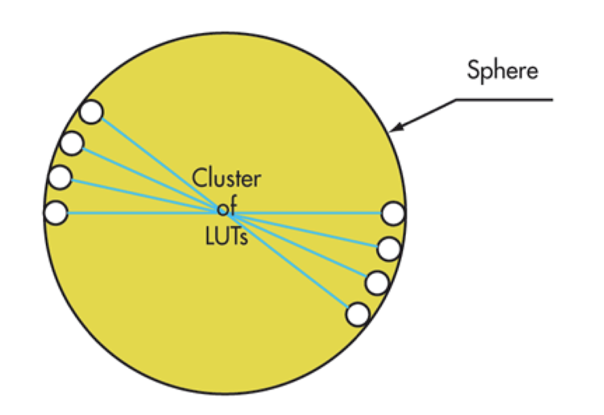
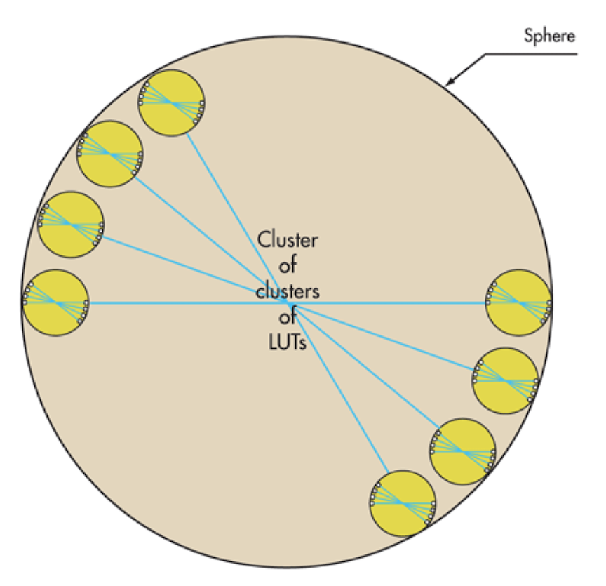
Meta systems took a custom FPGA based emulator approach. Instead of using off-the-shelf FPGAs, these companies manufactured FPGAs specialize for emulation. The base unit of these custom FPGAs was called a tile, and each tile contained a number of LUTs, reconfigurable switches between the LUTs, multi-ported memories, and IO interfaces, similar to a conventional FPGA. The tiles were connected hierarchically through a central crossbar that was time multiplexed. Because the inter-tile latency had very little variation compared to FPGA routing, where path delays vary widely, the compiler was able to achieve short compile times without spending time on extensive optimizations in synthesis and place and route. Meta Systems was acquired by Mentor Graphics and became the Veloce emulator.
FPGA Based Emulators (Excluding Synopsys and Cadence)
All existing emulator companies, excluding Synopsys and Cadence, are based on off-the-shelf FPGAs. The players include S2C, X-Epic, Oboe Emulation, BluePearl, Aldec, and others. These companies target different use cases. S2C supports fast turnaround times through incremental compilation and offers high performance with its in-house partitioner. Oboe focuses on a better debug experience by instrumenting the RTL to dump the full state. Aldec targets a specific design capacity range. Although many of these companies are profitable, and S2C, Aldec, and BluePearl have been around for a long time, it is hard to argue that they pose any real threat to the incumbents. To be honest, I am surprised that people use these emulators at all.
Repurposing ML Accelerator Chips for Emulation
The numerous emulator companies in the 1990s have now been replaced by ML accelerator chip companies. And on paper, these chips have characteristics that resemble emulation chips: large on-chip SRAM, huge amount of parallel processing, ability to scale compute across chips etc. Could it be worth building a compiler given a ML accelerator chip? Lets delve into the details.
Here are some characteristics that an hardware emulator should have:
- Independent instruction streams that can be processed in parallel
- Low latency on-chip communication, ideally via message passing
- Large SRAMs that can store the entire on-chip state as well as the intermediate computation results
- Low latency off-chip serdes
Here are the nice to haves:
- Narrow datapath (ideally less than 8 bits, my gut feeling is that 2~4 bit datapath is the best)
- High bandwidth off-chip memory for trace storage
Based on these criteria, we can evaluate various ML accelerators.
The MIMD Machines
Many of these AI accelerators resemble a MIMD architecture where PEs are programmed independently while communicating with each other through a message passing interface. Large on-chip SRAMs are also another condition that these chips satisfy. It already checks three of the four conditions that makes an architecture suitable for RTL simulation. Before jumping to conclusions, let us take a deeper look into each chip.
Tenstorrent Blackhole Tensix Processor

The base building block or PE of the TT cards is the TensixTile. A Tensix tile consist of five "baby" RISC-V cores where each core implements the RV32IM set. Each of these cores can be programmed independently of each other.

Each core is a typical pipelined RISC-V in-order core. For machine learning workloads, these baby cores are used mainly to push instructions to the Tensix coprocessor, or push messages over to another TensixTile. Each Tensix coprocessor is the big AI compute unit that contains:
- 2x Unpacker, for moving data from L1 into the coprocessor
- 1x Matrix Unit (FPU), for performing low precision matrix multiply-accumulate operations and some other matrix operations
- 1x Vector Unit (SFPU), for performing 32-wide SIMD operations on 32-bit lanes, including FP32 multiply-accumulate operations
- 1x Scalar Unit (ThCon), for performing integer scalar operations and 128-bit memory operations against L1 (including atomics)
- 4x Packer, for moving data from the coprocessor back to L1
The L1 cache has 1536KiB of RAM which backs the L0 instruction and data cache of each baby RISC-V processor as well as the coprocessor.

The chip contains 140 TensixTiles connected via a 2D-torus NoC topology, along with 16 SiFive RISC-V application cores.
Intuitively, mapping RTL simulations onto this architecture would look like the following. The circuit should be partitioned using a RepCut style graph partitioner. Each partition that gets mapped onto a TensixTile will be stored in the L1 cache. At the start of a dut cycle, each baby RISC-V core starts traversing the graph by loading in the state from the L1 cache and writing the intermediate results to it. Communication between the cores within a tile happens through the L1 cache. Cross-tile communication happens through the NoC by passing messages using the mailbox interface.
Using word level operations presents a favorable tradeoff compared to using LUTs in this architecture. Mapping the netlist into LUTs will increase the number of instructions for each processor to execute, as the LUT outputs must be concatenated and the RISC-V cores lacks the bit-manipulation instructions. Furthermore, it will put more pressure on the L1 cache read bandwidth as lookups must happen more frequently.
Supporting SRAM emulation is rather simple in this architecture as the processors can execute arbitrary code. Hence, it is possible to map each target SRAM bank as a software dictionary which significantly reduces the implementation cost, as well as removes the need to preallocate on-chip SRAMs for this purpose.
Adding waveform support also seem easier than other architectures. Once a snapshot period is reached, the L1 cache states of each tile can be flushed to DRAM. The snapshot can be shipped to the host asynchronously while simulation advances.
Back of the envelope performance projection:
- Assume 100K word level nodes
- Distributed over 720 processors
- 138 nodes per processor
- 10~15 pipeline stall per node (my assumption, L0 d-cache hit takes 2 cycles)
- 1380 ~ 2070 host processor cycles per dut cycle
- @1GHz frequency
- 500 ~ 700KHz emulation frequency
Back of the envelope capacity:
- Each instruction 4B
- Each node is 10 instructions (guessing) + produces one 4B word
- 44B per node
- 1536 KiB L1 = 34 * 1024 nodes per tensix tile = 34 K nodes per tensix tile
- 34K * 140 = 4M nodes
- Since this is word level, 4M nodes may be decent (not really sure)
Miscellaneous:
- The system can be expanded to multiple boards as it supports inter-board communication via QSFP ports
- The card is highly accessible. Anyone can purchase it for $1000
- Most of the chip area is wasted as the baby RISC-V cores take only 2% of the overall chip area2. Not sure how to use the coprocessor efficiently
Overall, out of all the ML accelerator chips, this seems like the most reasonable architecture. Especially because these are simple RISC-V cores, we get the software toolchain for free. This is easy to overlook, but actually very powerful.
PEZY-SC
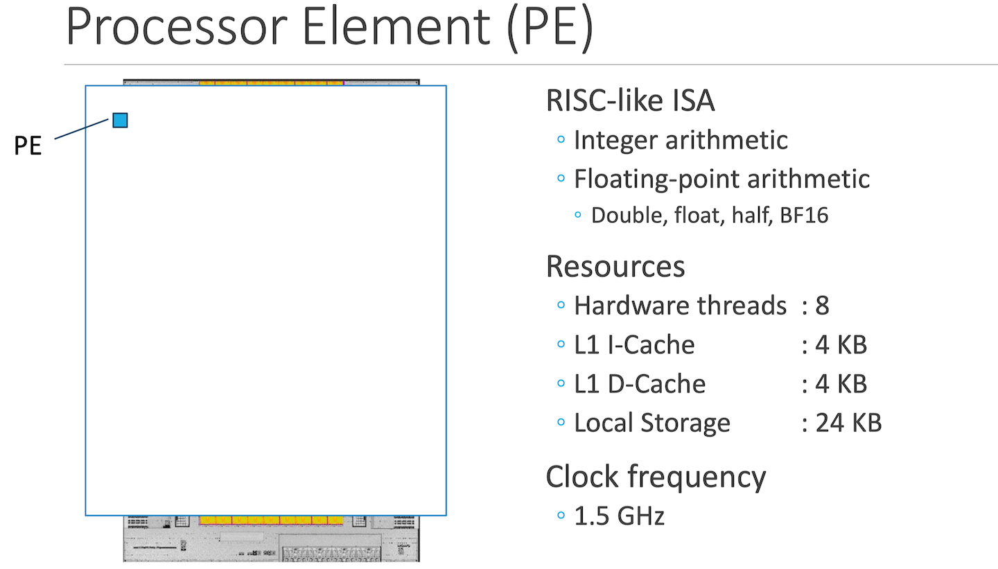
Each PE contains eight hardware threads, where each thread executes a a RISC-like ISA3. The hardware threads are grouped by fours, where the groups are switched when a thread encounters a long latency operation. Similarly, within a group of four threads, on a pipeline stall, threads switch execution. As latency is hidden via coarse and fine grained multithreading, each thread does not implement branch prediction.
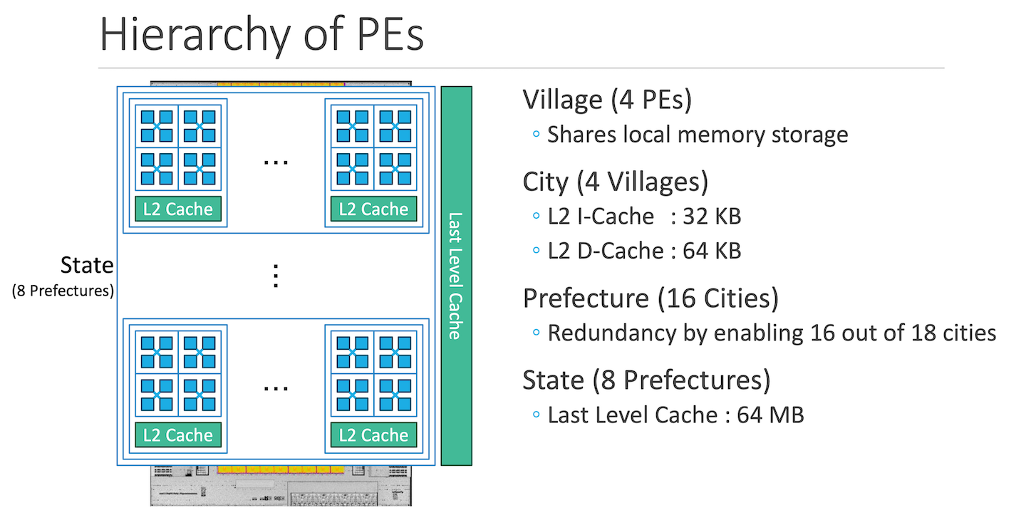
Each PE has 4 KB of L1-I & L1-D cache. A group of 4 PEs share a local memory of 24KB. In total, the chip has 200MB of on chip SRAM.
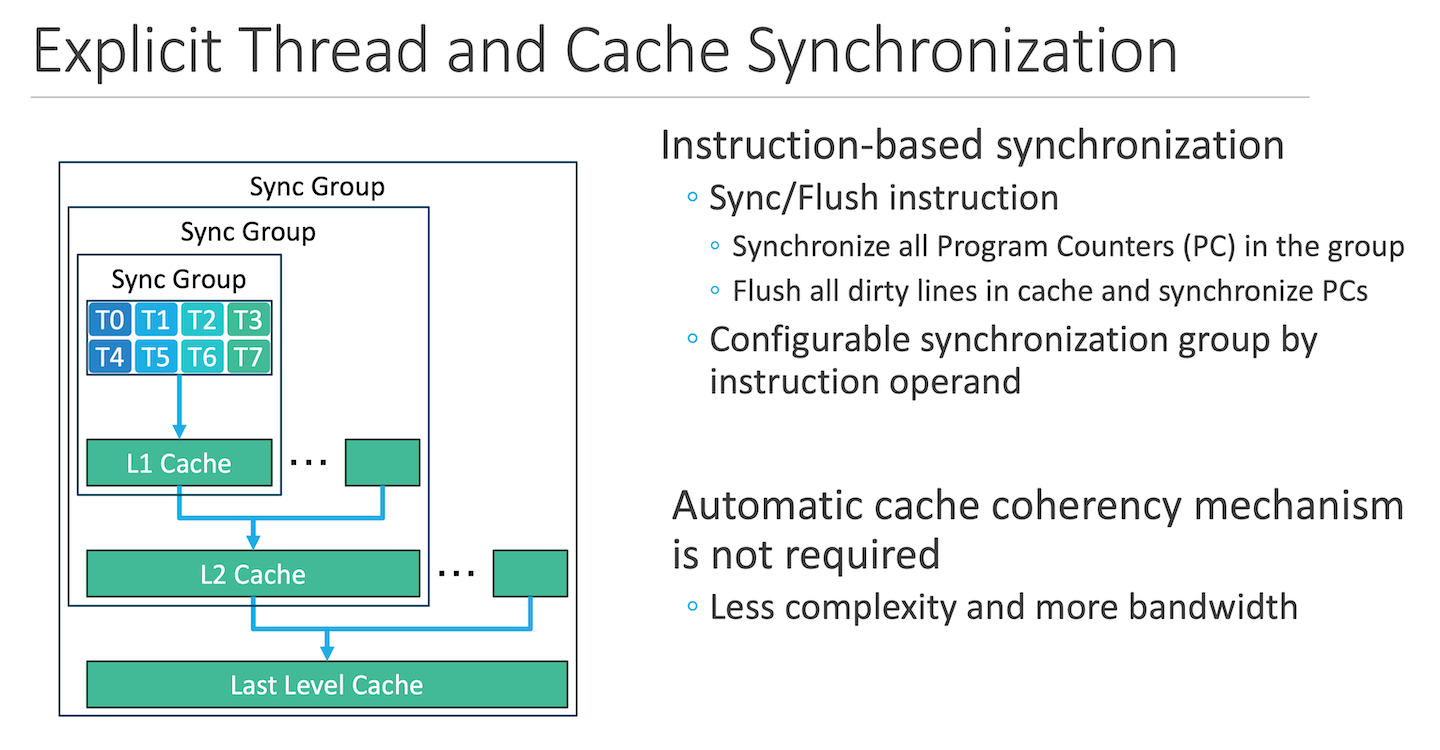
The memory subsystem is non-coherent, which means that cache flushes are required to share data between threads in different synchronization groups. For instance, if two cities within a perfecture wants to share data, it must execute a flush instruction. This will flush all dirty lines in the L1 to the L2 cache.
In terms of mapping RTL simulations on this architecture, the overall idea is similar to TT blackhole. Map parts of the word level netlist onto different PEs and use memory to communicate between PEs. The downside is that this architecture seems to lack a message passing interface between PEs, forcing cache flushes when trying to share data. The impact can add up, hurting performance. Furthermore, the PC synchronization mechanism implies that the program being executed by the PEs are identical. This itself disqualifies the architecture from being used as an emulator platform.
Miscellaneous:
- It has off-chip HBM, making it easy to support tracing
- Not having access to the low-level ISA could be problematic. Using OpenCL to program this to run RTL simulations is going to be a challenge
- It has no inter-chip communication link. To expand capacity, it will have to use the backing HBM to store state which is a huge performance penalty as now the performance will be memory BW bound
- Getting access to these chips seem impossible
Cerebras WSC
Each core, again is a simple in-order scalar processor with 48KB of memory.
NoC is a 2D mesh. 24 different independent static routes can be time multiplexed across a physical link.
The wafer has a total of 850K cores and 40GB of on-chip memory.
Similar to Tenstorrent, word level mapping of the RTL netlist seem reasonable. It supports arithmetic, logical, ld/st, compare and branch instructions which is enough to implement a word-level RTL interpreter. In contrast, the per-processor memory is limited (48KB vs 300KB). Any non-trivial design will have to be smeared across a large number of cores, resulting in a lot of cross-core communication.
The small number (16) of general-purpose registers, could also be a potential problem. This is tolerable for dense ML workloads where the scalar core register pressure isn't an issue. For generic RTL, register pressure turns into load and stores, larger program footprint, and lower performance.
There is no off-chip DRAM interfacing with the wafer, which means the traces must be stored somewhere on chip and streamed to the host.
As a side note, I urge readers to take a look at their programming model. It is by far the best software stack that exists for a non-SIMT chip, which also says something about their ISA. A notable feature is CSL's comptime construct. It enables the programmer to describe generic compute algorithms, and set kernel arguments once the problem size is determined. This should enable the software to adapt quickly, instead of being written specifically for a problem size. For this to work with RTL simulation though, to generate a per-processor program, one would require a metaprogramming layer on top of CSL.
Groq LPU
On surface, the Groq LPU seems decent because it has a large amount of on-chip SRAM and supports inter-chip scaling.
However, once one looks closely at the Groq architecture paper4, it becomes clear that it is a 144-wide VLIW machine with 20 vector lanes, which the paper refers to as superlanes. I will not go into the detailed microarchitecture of the LPU, but it is enough to say that the memory slices can be repurposed so that the read operations act as LUT lookups.
Again, without going deep into the microarchitecture, the anticipated problems are:
- A vector machine is not suitable for RTL simulations
- Expecting to keep all 20 lanes utilized without inserting a significant amount of NOPs for a generic RTL design is unrealistic
- It may work better when there is a lot of duplicate logic, similar to the Groq vector lanes themselves, and when the compiler can schedule that duplicate logic across lanes at the same time
- The way LUT readouts are streamed from memory to the compute units, and the way the LUT outputs are concatenated, requires very precise placement of the LUTs across different memory slices within a superlane. This serializes the lookup and reduces emulation throughput
- There is no off-chip DRAM, which means that in order to support waveforms, the chip must halt and transfer the register and SRAM state over PCIe. This significantly reduces performance, although it can be mitigated by taking periodic snapshots and replaying them on the host software simulator.
- The usual capacity estimate of total on-chip SRAM divided by the storage required for a LUT is overly optimistic. There are intermediate LUT outputs, intermediate addresses, register state, trace state, and other data that must be stored as well.
Of course, I could be wrong, and with heroic compiler engineering, one might achieve decent performance and capacity.
The Rest
If the architecture resembles something like a scalar core driving a big vector and matrix unit, it just won't work as an RTL emulator. TPUs, Trainium & Inferentia, and Etched are all in this category.
What it Takes to Compete
Then what is the slingshot that one should equip before going into a fight with the incumbents?
The obvious axis would be emulator throughput or capacity. However, this would be a fool's errand. The biggest customers of Cadence and Synopsys demand that their emulators become larger and faster every generation. In order to retain or increase market share, these companies put a great deal of effort into optimizing exactly these aspects.
Competing on cost is not promising either. Some AI chip companies will eventually fail, and their hardware may become cheap or even free. One might imagine building a compiler for those chips and selling inexpensive emulators. As discussed in the previous section, a repurposed piece of hardware will fall short in most cases5. More importantly, a serious chip company will not cut corners on emulation. If a customer chooses a low quality emulator only because it is cheap, that customer will not last long, because their projects will not survive.
The one area where the incumbents are not forced to improve is the quality of the user experience. Large chip companies are filled with engineers who have been using the same tools for years and no longer notice how poor the experience is. Anyone familiar with the progress made in software tooling and modern programming languages will see how far behind hardware tools are. Developer ergonomics, such as good LSP integration and static type checks, are easy to overlook. Yet in practice, they matter more than anything else. With better tools, engineers focus on their work rather than fighting the tools.
Modern programming languages also provide fine grained incremental compilation. If a language lacks this capability, it is simply not adopted. Although hardware development is fundamentally different from software development, the tools should still aspire to reach the same level of responsiveness.
Hence, I would argue that the most important metric for any RTL simulation or emulation company is compilation time. It is not enough to support the coarse-grained incremental compilation found in Vivado or VCS. Small edits to the RTL should result in compilation times of perhaps less than a minute. Once this standard is met, improving simulation performance and adding emulation support becomes much more straightforward. Achieving this requires rethinking the hardware intermediate representation so the compiler can identify stable regions across revisions, reuse previous results, and patch only the affected areas. Such an IR would also demand a new frontend language designed to integrate with it cleanly.
I agree that all of this sounds vague, but it matches a pattern repeatedly seen when new tools are adopted. Rust replaced C in many performance critical systems. Typst is overtaking Latex. uv is replacing conda and pip. LLVM replaced bespoke compiler back ends. Nix replaced various environment managers. In each case, the legacy tool was sufficient to get the job done, yet the new tool was better in many small ways because it was built from first principles. The improvements compounded until the old workflow became intolerable.
Verilog, SystemVerilog, and the current CAD tools are suitable for getting the job done, but they are far from being pleasant to use. Anyone who claims otherwise has either grown numb to the pain or never noticed it. A new CAD company that hopes not merely to survive but to succeed must place user experience at the center of its vision. Otherwise, it will join the long list of failed CAD startups.
x86 Multi-Core
That being said, the most practical platform for RTL simulation and emulation is the multi core x86 machine. It is already well understood on how to achieve near linear speedup with more cores when compared with VCS or Xcelium. Support for waveform tracing and non-synthesizable RTL is also far easier to build on a CPU than on custom hardware. And every design house already owns racks full of these machines.
For these reasons, the first product a new CAD company should build is an RTL simulator that scales its throughput with the number of cores and is powered by a compiler designed for incrementalism from the beginning.
References
We refer to simulation as something that supports full waveform dumping, arbitrary clock ratios, and 4-state simulation. Emulation lacks or has limited support of these features.
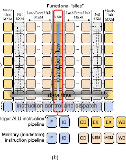
This is a terrible architectural diagram by the way. Until someone from the Groq team explain this to my friend who explained it to me, I was very confused after reading this
The perception that logic dedicated to instruction fetch can dominate the chip area is simply wrong. The correct architectural tradeoff is to always dedicate a little more area to make it more programmable
It's surprising that they decided to roll their own ISA instead of using RISC-V
Perhaps TT Blackhole has a chance